

Most of newer ADCs and DACs tend to use the JESD204b/c standards simply due to higher performance requirements – the ever growing need for more usable bandwidth, faster ADCs and DACs with increased resolution per sample and multi-channel implementations. The JESD internally uses Gigabit transceivers (Or MGTs – Multi Gigabit Transceivers ) with speeds of up to 32 Gbit/s per single lane (Xilinx Ultrascale + FPGA). This is indeed much higher than the older LVDS standard can handle. LVDS is in most cases limited to 1.6 Gbit/s per single pair (Xilinx Ultrascale+ FPGA), but reaching this speed is not easy and requires an extra care designing such an interface. Because 1.6Gbit/per pair (Or more realistically approx 800Mbit/s per pair) is not usually nowadays sufficient, more LVDS pairs tend to be used for a single interface. This differentiates the ADCs/DACs into Serial and Parallel. In Serial LVDS interface, the data word is transmitted within multiple bit clock periods based on the serialization factor, while in parallel implementation, the data word is transmitted via multiple lines at approximately the same clock speed as is the sampling rate of the device (May differ though).
What is also quite common is the usage of DDR LVDS (Double Data Rate LVDS), which reduces the clock speed by a factor of 2. Therefore 800 Mbits/s requires a bitclock of 400 MHz. In this mode, data are sampled on both the rising and falling edges of the bitclock. The 400 MHz frequency is also quite reasonable for the FPGA, as with newer technology, the FPGAs can reach speeds of 500 MHz +,but this on the other hand may complicate the internal design and requires some optimizations to meet the timing inside the Chip. Therefore 400 MHz is a good compromise between speed and design complexity (At least for Ultrascale+). The other commonly used standard is SDR LVDS (Single Data Rate LVDS), where the data are sampled on each rising (or falling) edge of the bitclock. In this mode the transmission rate and the clock rate are the same.
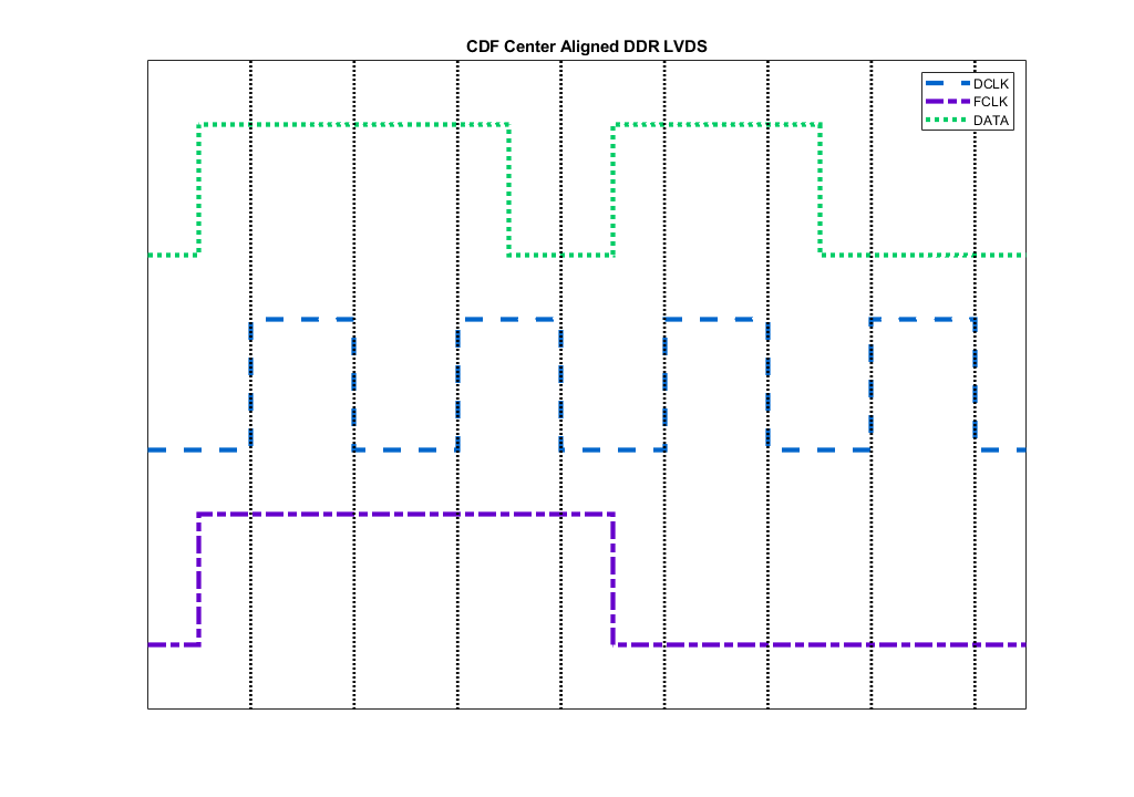
What is important for reconstruction of the data word at the receive side is the data format, or container (Usually denoted as CDF: Clk + Data + Frame). Here, Clk is the Bitclock, Data is the data sent and Frame denotes the boundaries of Words for successful deserialization of the words. ADCs and DACs have different CDF specifications for their modes, so that each time, the designer is responsible for properly aligning the data words to the frame boundaries. Below is an example of the CDF for DDR [Frame = 1,1,1,1,0,0,0,0],[Data = 1,1,1,0,1,1,0,0].
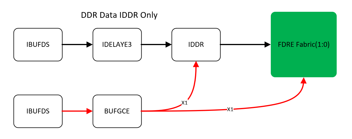
Capturing interface on the FPGA side can be made via a so called “Component Mode” or “Native mode“. The component mode is approximately the same as in the 7000 series devices (With limitations, but the topology is identical). On the other hand, the Native mode supports higher data rates (1600 Mbit in native vs 1250 Mbit in component ) and support features such as auto calibration of the interface. The native mode has also a dedicated clocking mechanism inside the IOB, which cannot be used in component mode. Though Xilinx recommends to use the Vivado’s HSSIO IP (High Speed Select IO Wizard),it not required to use it and the native mode interface may be instantiated inside RTL in a similar way the Component mode is instantiated there.
LVDS Component Mode Clocking
First of all, for proper FPGA clocking needs to be used a Clock – Capable pin (Usually denoted as: GC “Global Clock” ). These pins have dedicated routes to global clocking network inside the FPGA. What’s worth to mention as well is that not all FPGA banks support LVDS standard, for example HD (High Density) banks doesn’t support LVDS while HP (High Performance) banks does. Additional recommendation is that all the Data, Frame and Clock are located within a single bank and not distributed in multiple FPGA banks. Though this is not required, its basically highly recommended as it avoids some design problems.
The easiest method of clocking the IDDR or SERDES is via a global clock buffer. In fact all of the clocking options in component mode do require a global clock buffer clocking, but this specific clocking mechanism should more likely be called a Direct Clocking. That is that the clock from the GC pin is routed to global clock buffer and distributed to all IDDR/SERDES. In case of SERDES capture, there needs to be used a Clock Buffer with internal divider based on the required deserialization factor (IE BUFGCE_DIV in Ultrascale+).
One of the other options is to use a PLL or MMCM. This has some advantages over Direct clocking. At first, the internal VCO inside the PLL/MMCM is compensated for PVT (Power, Voltage, Temperature) variations, which makes sure, that proper clocking is applied across different operating ranges of the device. Both the PLL and MMCM can also serve as jitter cleaners, which may further stabilize clocking, not to mention, that the MMCM can also deskew the clock. And at last, the internal fine phase shift allows for compensation of different route lengths on the PCB. This can be adjusted as well by the IDELAY components, but when IDELAY is used for clock, the IDELAY output cannot be routed to global clock network. Basically, I prefer using the IDELAY since it adjust the data delay on per-pair bases.
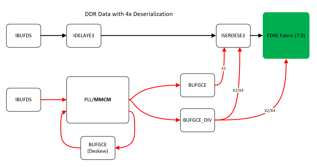
The designer may use the Xilinx’s Clocking wizard, but I always prefer to figure out the correct configuration myself and setup the internal dividers as needed. Information about PLL (Phase Locked Loop) / MMCM (Mixed Mode Clock Manager) configuration may be found in Xilinx’s UG572. One has to take care of the VCO’s operational range, this is specified in DS925 for Ultrascale+, and is between 800 and 1600 MHz. Note that when using the ISERDES, the bitclock needs to be divided by 2 (DDR deserialization 4 times or SDR deserialization 2 times) or by 4 (DDR deserialization 8 times or SDR deserialization 4 times). In case of using the ISERDES, the build-in FIFO inside the IOB could be used for synchronization between the 2 clock domains. The SERDES is likely required for data rates above approx 1Gbit/s.
Deserialization and Frame Alignment
After Successful capture of data bits via IDDR or SERDES, the data word needs to be reconstructed. This is usually simpler in case of parallel LVDS since differential pairs represent the bits of the data words. In case of Serial LVDS, one has to take care, whether LSB or MSB of the data word is sent first. In case LSB is sent first, the Word needs to be reconstructed from LSBs. The same applies for MSB-First mode. What is however even more important is that the data word needs to be aligned to the Frame boundaries. Below is an example of how the data word is sent from the ADC in LSB-First mode.

If the ADC clock would start synchronously with the deserialization inside FPGA,there would be no need to align the data to frame boundaries. But because either the FPGA or ADC clock starts asynchronously at random time, the data are likely deserialized such that the deserialized data word contains usually 2 ADC words instead of one. The Ideal capture of the data word is depicted below. Take an extra look at the time when the data bits of the words are sampled (LSB First Mode).

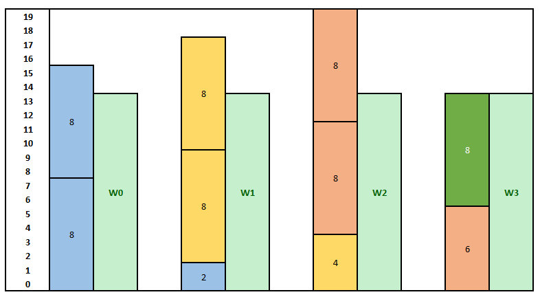
As was just mentioned, the deserialized word needs to be aligned to Frame boundaries. This can be implemented in several ways. In the previous 7000 series devices,there is a feature called bitslip – in case the data coming from SERDES were not aligned, then some RTL logic FSM would trigger a bitslip operation to delay the data inside SERDES by 1 bit (See UG471). This would loop until the deserialized data word was properly aligned to Frame boundaries. In Ultrascale+, there is no bitslip, so that the data needs to be aligned manually. This can be done for example in case of IDDR (Input Double Data rate Register) in such a way, that the deserialization FSM waits for Frame boundary (Usually transition from 000… to 111…). What I believe is a more robust solution however is to wait for 2 consecutive deserialized words and then do the alignment. This is depicted below.
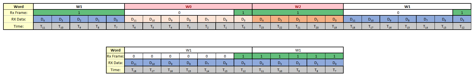
The left upper part (12b) is the deserialized word received at (T – 1) and the right upper part (12b) is the deserialized word received at time (T – 0). It can be seen, that these 2 12-bit words contain in fact 3 partial pieces of the ADC/DAC words. The W2 word is the word just being transmitted from the ADC, but its not yet fully transmitted at T – 0 and its bits are useless for alignment. Similarly, the W0 word is not complete and its previous bits are already discarded. What can be done however is the reconstruction of W1 word. In this situation, the 5 LSBs were already received at time T-1 and the rest has been received at T – 0. Therefore, the Word is aligned in the bottom as concatenation of the 2 parts of the deserialized 12-bit words. Once aligned, it can be considered static until either the deserializer or clock of ADC is reset. To be more precise, this is in fact a Barrel-Shift Register implementation (Basic concept is shown below: )
process(Clk)
begin
  if rising_edge(Clk) then
      case Frame is
        when "000000111111" =>
        when "000001111110" =>
        when "000011111100" =>
        when "000111111000" =>
        when "001111110000" =>
        when "011111100000" =>
        when "111111000000" =>
        when "111110000001" =>
        when "111100000011" =>
        when "111000000111" =>
        when "110000001111" =>
        when "100000011111" =>
      end case;
  end if;
end if;
At last, I would just love to add, that depending on the required deserialization factor, not all capture techniques may be optimal. For example, if the factor is 12, it doesn’t make much sense to use 8-bit deserialization, since additional logic will be required to properly deserialize the words. Furthermore whats likely more important is that in some cases (For example deserialization by a factor of 14). The deserialized data words will not be available at a constant period, which may cause some problems to DSP pipelines, which usually expect a valid sample each x periods:
In the Image above, data are coming from SERDES in 8 bits. We need to deserialize into 14-bit words. Therefore W0 needs to wait for 2 8-bit samples. After W0 is released,we have still 2 bits available for next word W1, but we still have to wait 2 8-bit words until we are able to deserialize into W1. Similarly for W2 – also have to wait for 2 8-bit words from the SERDES. But After W2,we have available 6 bits, so that in order to release W3, we only need to wait for the next SERDES 8-bit sample. Therefore the period is not constant and varies between 1 and 2.
An example of 14b deserialization FSM for both LSB & MSB-First modes (IDDR) is given below:
----------------------------------------------------------
------- Deserialization to 14-bit Words inside FPGA ------
Deserialization_14B_IDDR:process(Clk)
begin
  if rising_edge(Clk) then
    Data_Word_Vld <= '0';
    if Rst = '1' then
      State <= State_0;
    else
      ----------------------------------------------
      ------- DATA IS SENT IN LSB FIRST MODE -------
      if LSB_FIRST = '1' then
          case State is
            when S0 =>
              Data_Word(1 downto 0) <= IDDR_DATA;
              State <= S1;
            when S1 =>
              Data_Word(3 downto 2) <= IDDR_DATA;
              State <= S2;
            when S2 =>
              Data_Word(5 downto 4) <= IDDR_DATA;
              State <= S3;
            when S3 =>
              Data_Word(7 downto 6) <= IDDR_DATA;
              State <= S4;
            when S4 =>
              Data_Word(9 downto 8) <= IDDR_DATA;
              State <= S5;
            when S5 =>
              Data_Word(11 downto 10) <= IDDR_DATA;
              State <= S6;
            when S6 =>
              Data_Word(13 downto 12) <= IDDR_DATA;
              Data_Word_Vld <= '1';
              State <= S0;
          end case;
      end if;
      ----------------------------------------
      -------- DATA IS SENT MSB - FIRST ------
      if MSB_FIRST = '1' then
        case State is
            when S0 =>
              Data_Word(13 downto 12) <= IDDR_DATA;
              State <= S1;
            when S1 =>
              Data_Word(11 downto 10) <= IDDR_DATA;
              State <= S2;
            when S2 =>
              Data_Word(9 downto 8) <= IDDR_DATA;
              State <= S3;
            when S3 =>
              Data_Word(7 downto 6) <= IDDR_DATA;
              State <= S4;
            when S4 =>
              Data_Word(5 downto 4) <= IDDR_DATA;
              State <= S5;
            when S5 =>
              Data_Word(3 downto 2) <= IDDR_DATA;
              State <= S6;
            when S6 =>
              Data_Word(1 downto 0) <= IDDR_DATA;
              Data_Word_Vld <= '1';
              State <= S0;
          end case;
      end if;

    end if;
  end if;
end process;
Bit Alignment
Proper bit alignment means that the data bits are captured, when they are stable – IE in the middle of the valid period. There are two commonly used types of timing diagrams with respect to the bit clock. Either the data are edge-aligned or center-aligned. Edge aligned means, that the data bits change on rising and falling edges (DDR) and Center-aligned means, that data change their values with a 90° deg shift with respect to the clock. Usually, in case of edge-aligned interfaces, the receive clock needs to be shifted to the middle of the eye with a 90° shift on the clock itself. On the other hand, center aligned interfaces do not require additional phase shift on the clock signal.
The receive and transmit sides of the FPGA may delay the data bits by a small amount of time (Usually 0 – 1.1 ns) to compensate for length variations on the PCB among the LVDS PN pairs. It is still of course recommended to use matching lengths for the interfaces where possible (At PCB design level). In case of Ultrascale+ devices, there is also a possibility to cascade these IO blocks in order to delay the data by even larger amount of time (Again, see UG571 IDELAYE3 /ODELAY3 for more information). In the simplest form (or so called “COUNT mode” along with VAR_LOAD mode), the delay inside the FPGA may be modified on the fly. In combination with an ADC, that has a build-in test-pattern generator, one can estimate the middle of the valid data bit with respect to the configured delay value by looping across all the configurable delays (Taps) and measuring whether the received data changes overtime. This requires the test pattern to be constant (Any constant pattern except for zero pattern will do just fine) An example of such a sweep across all 512 taps is given below.
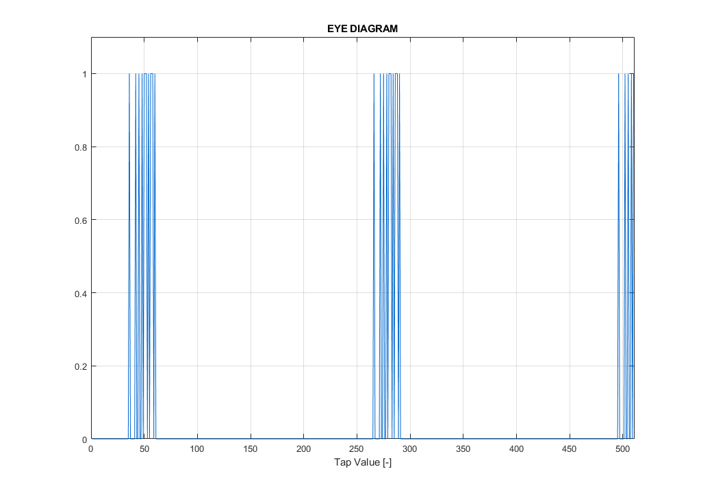
In this example, we see that based on the tap delay, we are able to properly align for the middle of bit 0 (Tap approx 150) and bit 1 (Approx 380). The choice is arbitrary if the frame alignment is implemented properly (via Barrel Shift for example). This specific result is however valid only for a single DATA pair. The same needs to be done for other pairs of the entire interface, including the frame itself. Be aware, that all of the signals needs to be shifted in the middle of BIT 0 or BIT1, but that these should not be mixed! Its also better to treat the frame signal as data signal and not as a clock signal – Use the same capture technique for both data and frame.
Native Mode
Native mode is a new feature in Ultrascale+ devices which includes the entire physical layer of the interface with improved calibration, management and includes a better clocking distribution inside the IOB. Because the clock is no longer routed through a global clock network, higher data rates are achievable in comparison with the older “Component mode”. The Build-in BISC (Build-in Self Calibration) ensures that data are sampled at the right time without any user intervention. The key to understanding the native mode is the hierarchy inside each HP IO bank:
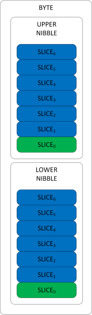
Each HP IO bank has 4 Byte Groups. Each byte group then consists of 2 Nibbles – the lower and the upper nibble. Each of these nibbles then contain 6 to 7 RX_TX_BITSLICES (Lower 6, Upper 7). What is important is that if any BITSLICE is instantiated somewhere in RTL, its automatically placed near the corresponding FPGA PAD. Therefore each PAD has its own BITSLICE. This is important as there are no other routes to or from other SLICES. Furthermore, each slice with index 0 can be used for clocking. (Eg. Clock must always be routed to any slice “0” FPGA PAD). There are basically only 3 types of these:
- DBC (Dedicated Byte Clock)
- QBC (QUAD Byte Clock)
- GC (Global Clock)
- GC_QBC (Combination – Routable to All Bytes and Global Clock network)
DBC may be used to clock the entire byte, but its route ability is limited to within the byte itself so that the clock cannot be distributed to other bytes of the same IO Bank. On the other hand QBC – capable pins may be used as clocking for all the bytes within the same IO bank. Furthermore GC pins are pins routable to global clock network. Most valuable is however the combination of GC_QBC pin,which is only one per entire IO bank. Clock from this pin may not only be distributed to the IO, but also to the global clock network. A very useful is the Xilinx’s website for pin-out specification of the ZYNQ Ultrascale+ devices: LINK.
Based on the required clocking, there may be some other requirements for the design:
- Inter-Byte Clocking (Clock from one Byte needs to be distributed to other Byte)
- Inter-Nibble Clocking (Clock from one Nibble needs to be distributed to the other Nibble)
The Inter-Nibble and Inter-Byte Clocking is managed via a dedicated routing mechanism available to the BITSLICE_CONTROL primitive. This primitive is associated with the corresponding slices. In case you find un-routable nets in the design, its likely that you are trying to connect BITSLICES to different SLICE_CONTROL ports (For example BITSLICE 1 to port 0 of BITSLICE control). Note that for differential interfaces such as LVDS, P and N signals have 2 pads, so that they also have 2 corresponding BITSLICES in the IOB. The data may be taken from the P-part of the interface only however. Based on the amount of required pads for the interface,there might be a need to connect NIBBLES and or BYTES together in order to build the interface properly. One may use the HSSIO wizard instead, but note that this wizard as of 02.2020 initializes the entire IO BANK and clocking across multiple IO banks is not supported.
Apart from all this, the recommended clocking tree is via PLL, which in Ultrascale+ has a dedicated clock route to all BITSLICE_CNTRLs (Port : CLKOUTPHY ). Additional options such as deserialization ratio, Delay format, Delay value and so on are accessible via RTL attributes. More on these may be found in UG571 under native mode description or in UG572 under PLLE4_ADV. The overall “Simplified” data and clocking chart is shown below:
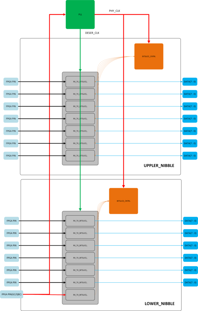
The red signal is clock heading from FPGA PIN (GC/QBC) to PLL and via dedicated PHY clock to both instantiated BITSLICE_CNTRLs. The green clock in this example is taken as PLL output as 1/4 Data clock due to DDR deserialization by 4 as the read clock to the build-in synchronization FIFOs inside the BITSLICES. The example shown also uses the BG2 (Bank group 2), HP Bank 66 of 7EV Device on the ZCU104 (Just for simulation purposes). RIU interface is not depicted and likely not needed for basic operation, though accessing the RIU though APB will likely not hurt anybody as well.
-------------------------------------------------
------- -------- BITSLICE_CNTRL_H ------- -------
--#AH8   IO_T2U_N12_66                       2U                 66    HP        NA
--#AG8   IO_L18N_T2U_N11_AD2N_66             2U                 66    HP        NA
--#AF8   IO_L18P_T2U_N10_AD2P_66             2U                 66    HP        NA
--#AG10  IO_L17N_T2U_N9_AD10N_66             2U                 66    HP        NA
--#AG11  IO_L17P_T2U_N8_AD10P_66             2U                 66    HP        NA
--#AH9   IO_L16N_T2U_N7_QBC_AD3N_66          2U                 66    HP        NA
--#AG9   IO_L16P_T2U_N6_QBC_AD3P_66          2U                 66    HP        NA
------------------------------------------------
------- ------- BITSLICE_CNTRL_L ------- -------
--#AH13  IO_L15N_T2L_N5_AD11N_66             2L                 66    HP        NA
--#AG13  IO_L15P_T2L_N4_AD11P_66             2L                 66    HP        NA
--#AJ11  IO_L14N_T2L_N3_GC_66                2L                 66    HP        NA
--#AH11  IO_L14P_T2L_N2_GC_66                2L                 66    HP        NA
--#AJ12  IO_L13N_T2L_N1_GC_QBC_66            2L                 66    HP        NA
--#AH12  IO_L13P_T2L_N0_GC_QBC_66            2L                 66    HP        NA
Additional info about constraining the Interface (Specifying input delay) may be found inside the Vivado templates under: Tools → Language Templates → XDC → Timing Constraints → Input Delay → Source Synchronous → Center-Aligned → DDR/SDR. Below is the copy from Vivado 2019.1, but always lookup the template in your own environment and Vivado version! Also remember, that even though the design may fail the timing on the input interface (Setup and Hold on ISERDES/IDDR), you may still be able to manually properly align the window via technique discussed earlier for example. Setting false paths on the input is however not recommended. Additional tip for manual dynamic calibration is to set all delay taps to zero(Initial Value), so that they are not included in the timing summary. Also make sure, that clock into the IDELAY matches the clock to the ISERDES(CLK_DIV)/IDDR. If these clocks are different, the IDELAY for the FPGA PAD is placed automatically to different PAD locations, which worsen timing.
Additional tip is to enable the on-die chip termination for the LVDS interface in case proper termination is not done by the PCB designer or if custom SOM module is used for the design. This can be done via GUI (IO Planning → DIFF_TERM_ADV →TERM_100) or manually via XDC such as: set_property DIFF_TERM_ADV TERM_100 [get_ports DATA_P[0]].
# Center-Aligned Double Data Rate Source Synchronous Inputs
#
# For a center-aligned Source Synchronous interface, the clock
# transition is aligned with the center of the data valid window.
# The same clock edge is used for launching and capturing the
# data. The constraints below rely on the default timing
# analysis (setup = 1/2 cycle, hold = 0 cycle).
#
# input                  ____________________
# clock    _____________|                    |_____________
#                       |                    |
#                dv_bre | dv_are      dv_bfe | dv_afe
#               <------>|<------>    <------>|<------>
#          _    ________|________    ________|________    _
# data     _XXXX____Rise_Data____XXXX____Fall_Data____XXXX_
#

set input_clock         <clock_name>;      # Name of input clock
set input_clock_period  <period_value>;    # Period of input clock (full-period)
set dv_bre              0.000;             # Data valid before the rising clock edge
set dv_are              0.000;             # Data valid after the rising clock edge
set dv_bfe              0.000;             # Data valid before the falling clock edge
set dv_afe              0.000;             # Data valid after the falling clock edge
set input_ports         <input_ports>;     # List of input ports

# Input Delay Constraint
set_input_delay -clock $input_clock -max [expr $input_clock_period/2 - $dv_bfe] [get_ports $input_ports];
set_input_delay -clock $input_clock -min $dv_are                                [get_ports $input_ports];
set_input_delay -clock $input_clock -max [expr $input_clock_period/2 - $dv_bre] [get_ports $input_ports] -clock_fall -add_delay;
set_input_delay -clock $input_clock -min $dv_afe                                [get_ports $input_ports] -clock_fall -add_delay;

# Report Timing Template
# report_timing -rise_from [get_ports $input_ports] -max_paths 20 -nworst 2 -delay_type min_max -name src_sync_cntr_ddr_in_rise  -file src_sync_cntr_ddr_in_rise.txt;
# report_timing -fall_from [get_ports $input_ports] -max_paths 20 -nworst 2 -delay_type min_max -name src_sync_cntr_ddr_in_fall  -file src_sync_cntr_ddr_in_fall.txt;
Overall, the native interface is very similar to the old component mode in way that it include all the components as well, but improves clocking tree, performance, features such as auto calibration and unifies the design topology. Though new in Ultrascale+, Native mode is “Quite easy” to understand – well, it needs some time, but here comes the great + for all the XIlinx’s data sheets: They are quite readable and you will likely not encounter much issues and or misunderstandings inside them. The designer is therefore no longer required to fully understand the interface itself and may concentrate or more important things such as going out for a walk with the dog or go cycling 🐾