

The times when designers used to calculate and adjust manually delays across PCBs to match a device’s requirements (Such as a memory or ADC/DAC interface) for a few megatransfers / second are definitely over nowadays. Even though they are still used on some prehistoric devices, they were replaced by advanced and more robust interfaces, which incorporated features like error correction, dynamic calibration and alignment. Not so long ago was Xilinx’s FPGA Ultrascale PHY redesigned in order to support DDR4 specification and bring higher data rates to the FPGA . Personally, I am sometimes really impressed by the ever-growing rates on all interfaces around us. My PC motherboard for example has PCIe Gen 3.0. I would say its still quite a new and definitely sufficient specification for all my computations and usage of my beloved Maxwell-based nVidia GPU. But the truth is that there is currently PCIe Gen 4.0 as a mainstream and there are devices on the market which also has support for PCIe Gen 5.0 not to mention, that Gen 6.0 PCIe is currently baselined on paper. The difference is huge, Gen 3.0 uses 8GT/s while Gen 6.0 is rated for up to 64GT/s per single lane. That is 8x increase in throughput over “just a few years”. If you are however not familiar with PCIe, the situation is the same with other common interfaces such as Display Port, Thunderbolt or even USB! Yes, even the bloody USB (At least 3.0) uses high-speed serial IO nowadays.
The importance of understanding the high-speed serial IOs is evident. To be honest, I am not the expert on this topic, but I believe that a good designer should at least know how it works, what are its limitations, requirements and especially be able to use such an interface and eventually debug why its not working. Even though using the HSSIO (High Speed Serial IO) or SERDES (Serializer – Deserializer) – commonly referenced as GTs or MGTs in general requires some knowledge, its at least for Xilinx’s quite good covered in the data sheets. I remember when I was asked some years ago whether implementing a JESD204b interface on 6 lanes, each rated at 15Gbit/s might be challenging. Personally, I wasn’t that much afraid that it wouldn’t work, since I do know Xilinx devices for quite a while … and so if I see that the SERDES interface is rated for up to 16.3Gbits/s in the datasheet, I do know, that unless I do make some stupid decision (Which I do occasionally unfortunately do), its very likely, that it is going to work especially on Xilinx’s boards used for development such as ZCU106 or VCU118.
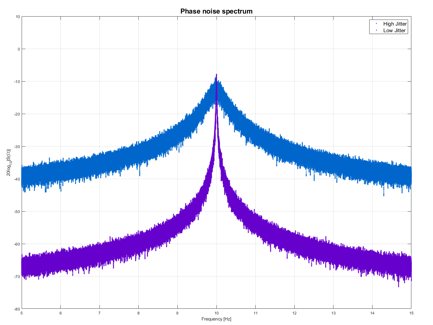
One of the key steps to ensure functionality of such interface is to pay extra attention to clocking of the transceivers. The clock must be stable, clean and must have a very good jitter specifications ( See example above). Note that “PPM” is something other than “jitter in ps/fs RMS” – although they are usually a little bit related (Higher ppm stability – IE small PPM – leads to better jitter specifications). The PPM defines the stability of an oscillator to stay at its nominal frequency (An oscillator at 100MHz and 200 ppm is allowed to drift by 100e6/1e6 * 200 = 20KHz in the range from [100M – 20K] to [100M + 20K]). The higher the ppm, the more is the source going to drift away from this frequency over time. Protocols such as PCIe include a clock correction sequences, which allows for small clock variations between RX and TX and consist of special control characters encoded in the data stream, that allow the receiver to compensate for these changes. Random jitter (Usually defined in ps/fs RMS) on the other hand defines the variation of a period of the clock signal and directly relates to the phase noise masks and phase noise. An example of such a mask for different reference clock frequencies is given below for GTY Virtex Ultrascale+ Transceivers ( Visit AC/DC Characteristic for the corresponding family: DS893 for Virtex Ultrascale+ and DS922 for Kintex Ultrascale+ for example):
| Carrier Offset: | 10 KHz | 100KHz | 1MHz | RMS Jitter |
| 153.25 MHz | -112 dBc/Hz | -128 dBc/Hz | -145 dBc/Hz | 448.3 fs |
| 312.5 MHz | -103 dBc/Hz | -123 dBc/Hz | -143 dBc/Hz | 507.3 fs |
| 625 MHz | -98 dBc/Hz | -117 dBc/Hz | -140 dBc/Hz | 467.5 fs |
The easiest way to calculate the RMS value is to use an online calculator such as RFTOOLS. By knowing the RMS value, one may choose a clocking solution, that satisfies the FPGA’s requirements. SiliconLabs (Among other companies, but SiliconLabs is my favorite so far – I am unfortunately not paid for this article neither by Xilinx, nor by SiliconLabs 👀 ) has a wide and proven range of very good and stable clock-generators to suit any high-speed serial interface. There is a brief AN699, which covers the clocking basics and recommends a clock generator family based on the calculated value. The GTM / GTX / GTH / GTY / (Or other GT Types) transceivers inside the FPGAs also have build-in solutions for debugging PCB issues of these serial interfaces such as the IBERT (Integrated Bit Error Ratio Tester) with the capability to optionally show an EYE diagram, but the need to use an eye diagram for debugging is likely due to a poor PCB design, bad clocking solution or problems due to PCB signal integrity in the first place.
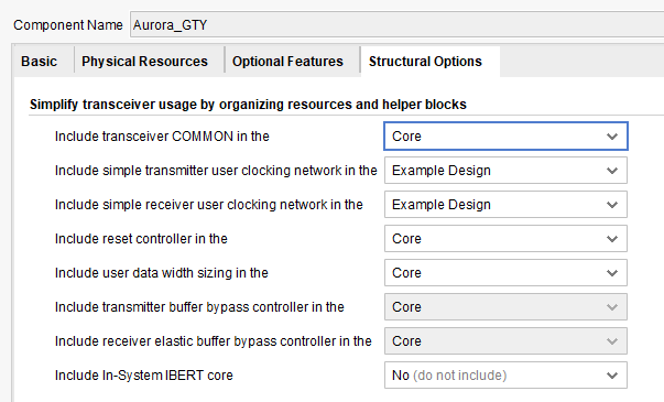
Nevertheless, this post should provide some intel on the Aurora 8/10B Interface. As it suggests, the usage of 8/10 encoder/decoder in inevitable here. When designing with the Transceiver Wizard (I have targeted for this purpose the VCU118 development board), one has to decide which SERDES data width to use. This can be either 16 or 32 bits for enabled 8/10B coding (And equals to Internal data width of 20 or 40 bits). The choice is irrelevant, the higher the bitwith, the slower the SERDES clock frequency. IE. I have prepared a GTY example on 4Gbit/s single lane in 32/40 Configuration. In this scenario, the SERDES clock is simply the lane rate / 40, which results in the RX or TX clock of 100 MHz. Be aware that these are the TXOUTCLK and RXOUTCLK clocking ports and should be “In most scenarios” treated as asynchronous. There is a possibility to use TXOUCLK for also clocking the RX part of the transceiver under special conditions. The Transceiver wizard by default uses the “Include user clocking network in example design” which I believe is the best choice you can make as you have complete control over clocking of the transceiver. I have also used the “Transceiver common in example design” option in one specific design, but I discourage you to do that unless necessary, since its a lot wiring without any added advantage to be honest (But still, you have to do that If you want several different interfaces located in the same GT quad). Also the transceiver requires a very specific reset scheme and although you may write your own reset sequence, I would also advice you not to do that and use the “Reset helper block in the core”. You can see details on the configuration below (I could have used the same PLL for both RX and TX, but I decided to use QPLL0 for TX & QPLL1 for RX. I tend to avoid using the CPLL and to be honest, I don’t know the exact reason, but it happens that your interface might require more lanes than just one and thus usage of a QPLL comes handy, as its shared for all the lanes and possible reduces board power).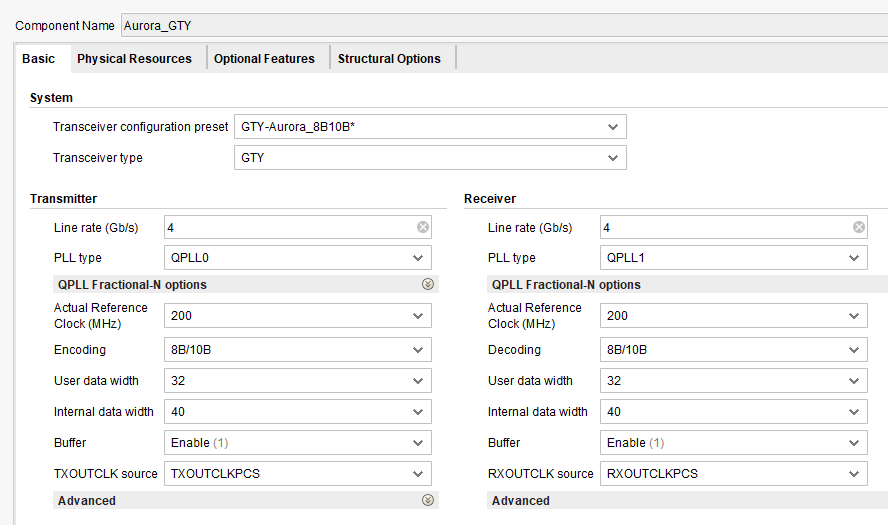
The clocking helper block substitution is simple and worth it. The only thing you need to take care of is whether ( _USRCLK2 == _USRCLK) or whether (_USRCLK2 = _USRCLK / 2). This can be easily found in the corresponding datasheet (UG576 for GTH transceivers or UG578 for GTY Transceivers) and looking into ” Interface data path Configuration”, where you find your own setup. The connection is easy thereafter and shown below. The optional division by two can also be done in the BUFG_GT primitive, which is nothing more, than a dedicated transceiver clock buffer with the optional possibility to divide the clock (For example by 2). As usual, the BUFG_GT is covered in the corresponding clocking manual for the family used (UG572 for ultrascale family).
![]()
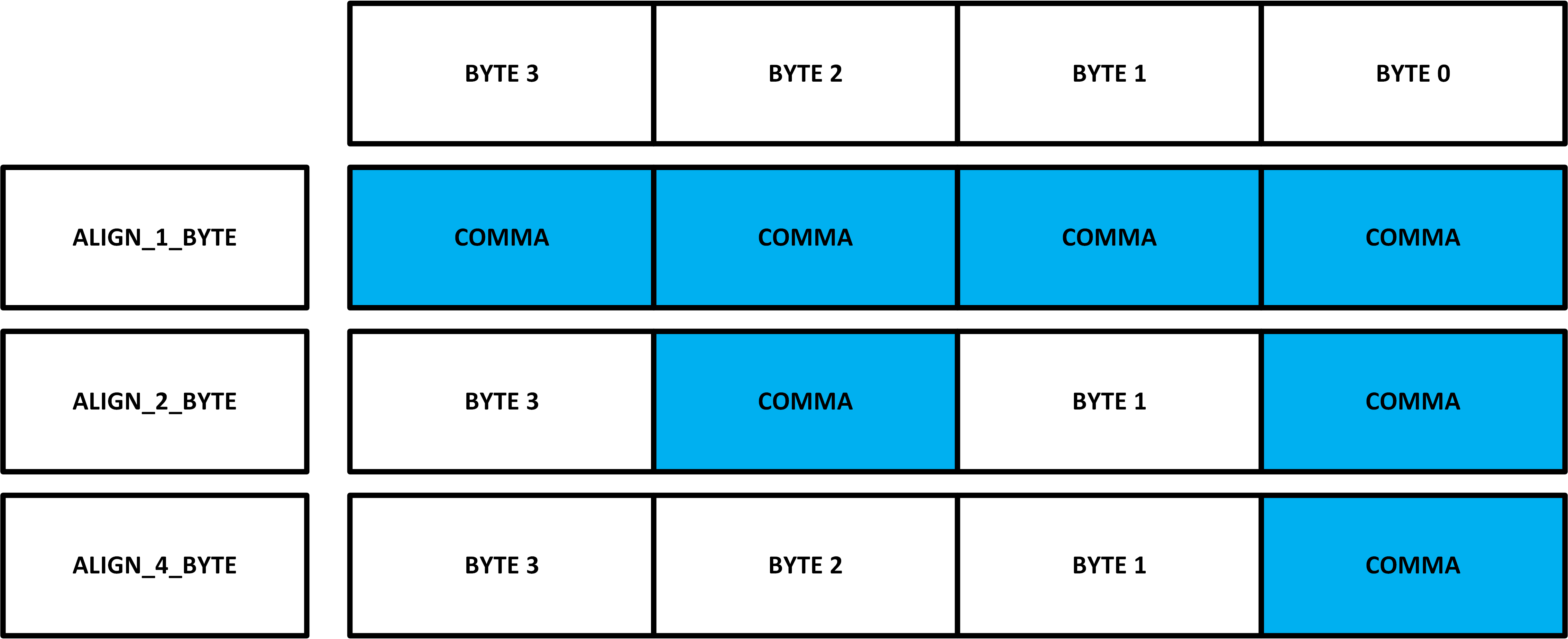
The most interesting part is however with the coding / serialization / disparity and usage of the control characters “K-Chars“. For Aurora, the 8/10 encoder and decoder blocks inside the transceivers should always be enabled. The control characters are a set of very specific symbols used for synchronization, alignment, clock correction etc. They have a unique property – no data can be mapped to symbols of the control characters. As I have noted before, my example uses serialization factor of 32. In order for the receiver to successfully decode the incoming data stream, it has to align itself to “some” boundary. This can be a 1-byte boundary / 2-byte boundary or 4-byte boundary. Because I have used 32b interface width and expect data to be 32-bit wide, the choice to align to 4-byte boundaries has been made. In order for the receiver to align, the transmitter has to send a “COMMA K CHAR” with a disposition and location as stated in the transceiver documentation with respect to the SERDES data width used. The receiver then searches for this comma-character and align itself with it. Based on the protocol, the transmitter should occasionally send these characters. The transceiver wizard allows for choosing the synchronization sequence (IE it doesn’t have to be a comma or K28.5 / K28.1, but these should be kept at default for most scenarios.)
The only note worth considering is the COMMA-P “K28.5+: 100000101″ and COMMA-M “K28.5-: 0011111010“ options under “Optional Features” of the Transceiver IP Wizard. These are the corresponding comma alignment symbols with respect to running disparity (RD). This is a technique used to maintain a zero DC of the transmitted data stream so that the Receiver’s CDR (Clock Data Recovery Circuit) can align to the data sequence properly. The GT Transceiver TX side allows for various modes of operation: It can force a negative disparity, positive disparity or “let the encoder decide whatever it wants “. The settings is based on txctrl0 & txctrl1 ports. Usually, the last option is what you want, IE. let the encoder decide about the running disparity. It however depends on the protocol specification. This affects the comma character specification. “COMMA-P” detects a positive running disparity K 28.5 / K28.1 character while “COMMA-M” detects the negative disparity of the same character. The entire control character set is specified for example in the UG576 / UG578. Of course, that if the protocol forces either of those disparity settings only, then the other one will not be detected. For a 4-Byte comma alignment, only one (Either positive or negative) alignment is required – IE, if the SERDES aligns on the positive, then the same alignment is also valid for negative. This is indicated by the “rxbyterealign” port of the transceiver. Until the alignment is completed, the transceiver will output all kinds of errors including wrong comma character detection, not in table errors or disparity errors.
In my example, I have used a single lane configuration so that no channel-bonding is required. In case the aurora interface is split between multiple transceivers, then the Aurora specification tells how data sequences should be split between the transceivers. In order to distinguish between the lanes at the RX, channel bonding “Or channel Recognition” sequence is required. This is however not covered in my simulation. In order to test the setup, a “simple TB” comes quite handy especially with the loopback, which is a part of all the GT transceivers. The loopback can be specified to “NEAR-END PMA“,”NEAR-END PCS“,”FAR-END PMA”,”FAR-END PCS”. PCS stands for “Physical Coding Sublayer” and PMA for “Physical Medium Attachment”. If you want a simple loopback from TX back to RX on a single GT, then “near-end” is what you want. The far-end testing requires 2 GT instances to operate in a single TB. The decision whether to use PMA or PCS depends, PMA is more of a real-life wire loopback since its closer to the physical medium. Furthermore, in order to test the PMA, one may use one among the supported PRBS (Pseudo Random Sequences). The RX is able to synchronize on the sequence and measure the BER (Bit Error Rate), which can be read through a DRP (Dynamic Reconfiguration Port) interface. I personally used this feature on the JESD204b 15Gbit/s per lane interface and it worked flawlessly.
As you can see from the waves, there is an initial reset sequence, where nothing really happens expect for a few reset-done signals, powergood statuses and CDR stable signals … This is followed by the “GREEN” rectangle, where the RX tries to comma align on the incoming data stream. You can see, that during the “P-COMMA” alignment, the alignment has changed and “Aurora_Align_Changed” signal is asserted for a cycle – telling us that the RX is comma aligned. The “M-COMMA” alignment follows and is completed without assertion of the alignment change as stated previously because the alignments are identical. After the sequence is completed, I manually reset the RX elastic buffer. The transceiver IP can be optionally configured to do this automatically whenever comma character is detected. The “YELLOW” rectangle then shows “A standard stream of data”, which is produced by the TX and successfully decoded by the transceiver’s RX side. The successful decoding is shown such that there are no disparity errors and also no “not-in table” errors – These would be the results of invalid 8/10 symbols from 8/10 decoder. I let the simulation run for 20us and then switched data source to PRBS which I highlighted in the last “WHITE” rectangle. As you can see, there is plenty of disparity/not-in-table errors, but since the data stream is sourced by a pseudo random sequence, these can be safely ignored. The only thing that matters at this moment is the “PRBS_Locked” signal, which is okay.
Tip: The simulation also uses a custom reset sequence, which resets the TX first and then RX. This is to help with the CDR’s locking at the RX, which preferably requires some traffic in order to lock properly. If there are no data coming through, then I may suggest to use the RXCDRHOLD transceiver pin tied high when RXELECIDLE is asserted so that the CDR will not pickup any noise. This is as well documented in UG576 / UG578.
At last, I am glad that the simulation works and everything is okay and the life is beautiful again (at least for a while 😇 ).
The entire project along with code coverage is available ➡️ HERE ⬅️.
IP is Targeted for VCU118 & Vivado Ver. 2020.2.