

The most basic setup of simulating/using PCIe on Xilinx FPGA / SoC devices is having a single endpoint (EP) and a single Root Complex (RC). One may accomplish this by instantiating only the base Hard IP Wrappers (Consisting of Physical Layer, Data Link Layer and Transaction Layer – Documented in PG213) in the TestBench and managing all the TLP packets and or messages in a custom user logic outside of the macro. This brings the greatest freedom at the cost of extra development time for the required functionality. For plenty of designs however, it may be more convenient to use an AXI to PCIe bridge optionally as well with the DMA (Documented in PG195) in order to improve performance and throughput. The XDMA IP in the AXI bridge mode as documented in PG194 creates a wrapper around the PCIe Hard IP itself and translates AXI & PCIe transactions in both ways. On the other hand, only a specific set of packets are supported by the bridge, these are AXI – Compatible. Non-Compatible AXI Transactions are not supported by the bridge. Both the Root Complex and the Endpoint may (But may not) have a slave (S) and master (M) side on AXI. Master Side is used for managing incoming transactions into the EP / RC while slave side is used for outgoing transactions away from the EP/RC. Both the EP and RC may therefore receive and send data, which comes handy if there multiple endpoint devices, which needs to communicate between themselves.
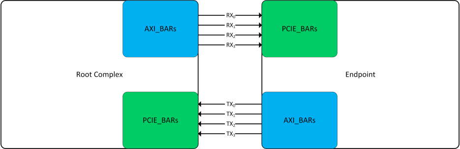
What one may wonder however is how PCIe Address space and AXI Address space are connected and or related. The simple answer is that they are not and that they have really nothing in common. We will now take a quick look at the processing of both incoming and outgoing transactions and parameters of the bridge that take place in processing them such as the address translation setting both from PCIe to AXI and from AXI to PCIe. In the example below, I have tried to show an example of communication from the “RC” to the “EP” (But note that PCIe is symmetrical and the same scheme may apply to communication from EP to RC with the exception, that RC may implement only one PCIE_BAR). The RC PCIe Bridge below Implements two AXI_BARS and the EP implements the same amount of PCIE_BARS. Now important is to understand that AXI_BARS are used for translation of an AXI Memory-Mapped address range into a PCIe address space while PCIE_BARS are used to translate PCIe address space into an AXI Memory-Mapped address space. Neither of these spaces has to be related and the choice of AXI MM ranges in both the EP and RC designs is arbitrary.
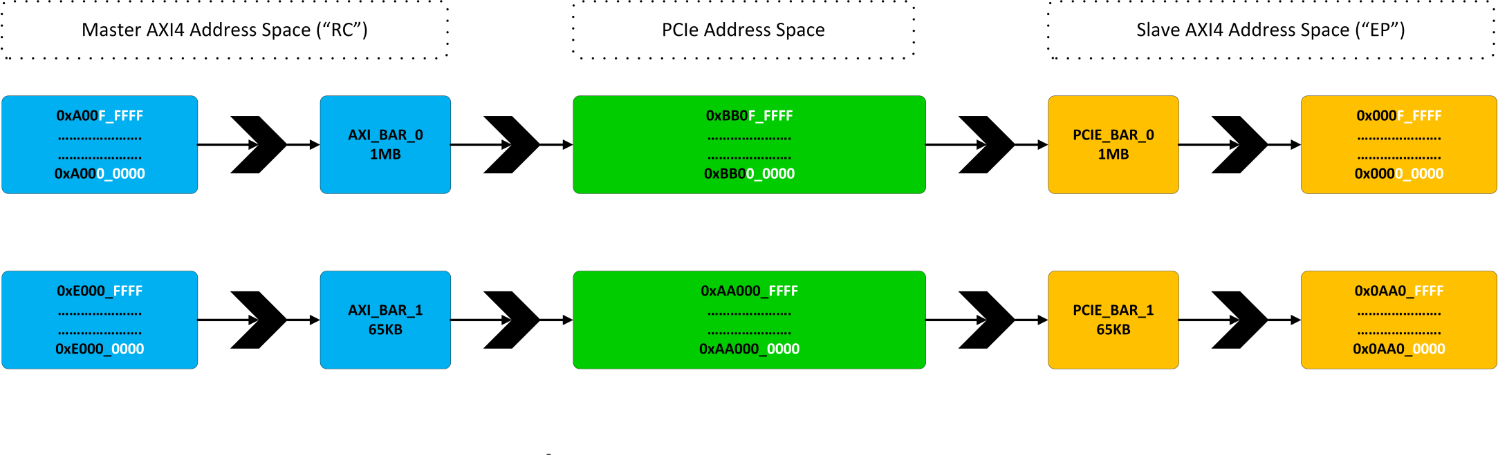
Any AXI4-Master in the RC design may initiate an AXI transaction to address within the range from 0xA000_0000 to 0xA00F_FFFF. Any read or write into this location is translated to PCIe Address range from 0xBB00_0000 to 0xBB0F_FFFF. This is a 1MB range. This Mapping is usually based on the RC PCIe topology enumeration and has been chosen as an example in here. The RC software should also setup correct PCIE_BAR settings at the endpoint during enumeration, which in this case matches PCIE_BAR0 at base address of 0xBB00_0000. As a result, any PCIe transaction in the range from 0xBB00_0000 to 0xBB0F_FFFF gets translated into the EP’s AXI MM address space – In this case chosen to be 0x0000_0000 to 0x000F_FFFF. The EP may of course use smaller and or larger BAR size then 1MB. If any PCIe transaction is however received outside the PCIE_BAR_0, then it is treated as a “BAR Miss” and such transaction is not propagated to the AXI Back-End. Note that PCIe enumeration is not responsible for the AXI Address ranges defined in the EP/RC designs and cannot change them (They remain constant). The same process applies to the secondary AXI_BAR_1 and PCIE_BAR_1 with the exception that different address ranges and BAR sizes have been used. Even though the AXI address ranges are constant, the target PCIe translation address maybe configured at runtime after enumeration (Continue reading).
Incoming Transactions (EP in Example Above)
As is shown, the PCIE_BAR0 is mapped into the AXI MM address range from 0x0000_0000 to 0x000F_FFFF (Size defined as PF0_BAR0_APERTURE_SIZE and translation defined as C_PCIEBAR2AXIBAR_0 ) and PCIE_BAR1 is mapped into the AXI MM from 0xAA00_0000 to 0xAA00_FFFF (Size defined as PF0_BAR1_APERTURE_SIZE and translation defined as C_PCIEBAR2AXIBAR_1). The endpoint allows for mapping of up to 6 fully independent 32-bit PCIeBARs (or up to three 64-bit PCIEBARs) that may have arbitrary AXI MM address mapping. The settings that are required to figure out which BAR lies on which AXI address are therefore the BAR sizes and PCIEBAR2AXIBAR mappings:
- C_PCIEBAR2AXIBAR_0 (0x0000_0000)
- PF0_BAR0_APERTURE_SIZE (1MB)
- C_PCIEBAR2AXIBAR_1 (0xAA00_0000)
- PF0_BAR1_APERTURE_SIZE (64KB)
Note that these settings affect only the incoming transactions to the Endpoint. If the corresponding BAR is hit, then a transaction at the mapped address is initiated. For example, a PCIE_BAR1 hit would be translated by the bridge to AXI Read/Write on address defined as: “Offset Inside the BAR” + 0xAA00_0000 (C_PCIEBAR2AXIBAR_1). Specifically, a PCIe write coming to the endpoint at an PCIe address of 0xAA00_1000 would be translated by the PCIE_BAR_1 to AXI write transaction with address of 0xAA00_1000. The address would not be changed in this case only because PCIE_BAR_1 configuration makes sure that PCIE & AXI address spaces are equal, which is of course as well possible. A write into PCIE_BAR_0 at 0xBB01_0000 would however result in AXI write transaction with a translated AXI address of 0x0001_0000.
Outgoing Transactions (RC in Example Above)
Similarly to PCIe BARs, one may define a number of AXIBARs, which translate AXI MM transactions into PCIe Transactions. As in the case of PCIeBARs, AXIBARs may lie on independent AXI address ranges apart from PCIe. For the example above, AXI_BAR_0 lies on address from 0x0A00_0000 “C_AXIBAR_0” to 0x0A0F_FFFF “C_AXIBAR_HIGHADDR_0” and each hit into this address range would be translated to outgoing PCIe transaction with address defined as “AXI_ BAR_0 Offset” + C_AXIBAR2PCIEBAR_0 translation mapping
- C_AXIBAR_0 (0xA000_0000)
- C_AXIBAR_HIGHADDR_0 (0xA00F_FFFF)
- C_AXIBAR2PCIEBAR_0 (0xBB00_00000)
Similarly for AXI_BAR_1, the AXI Address range starts at 0xE0000_0000 “C_AXIBAR_1 ” and continues up to 0xE000_FFFF “C_AXIBAR_HIGHADDR_1”. Any transaction in this range is then translated into PCIe Transaction at an offset of 0xAA00_0000 “C_AXIBAR2PCIEBAR_1”.
- C_AXIBAR_1 (0xE000_0000)
- C_AXIBAR_HIGHADDR_1 (0xE000_FFFF)
- C_AXIBAR2PCIEBAR_1 (0xAA00_0000)
AXIBAR2PCIEBARs (Translation from “RC” AXI Address Space to PCIe Address Space) are configurable via the bridge’s AXI4-Lite interfaces (Which is a must, since the enumeration done at the RC will map some PCIE_BARS in the PCIe topology to arbitrary address ranges, which in turn needs to be reflected in the translation registers). The PCIeBARS are configurable on the other hand with a standard PCIe Configuration write transactions (Either Type 0 or Type 1). Note that neither of these changes affect the internal design, but rather manages the interoperability across the PCIe topology with other devices. Any Slave or Master inside the Design sitting on any AXI address would still use the same AXI address regardless of whether the BAR base addresses have been changed by the root complex or whether the AXIBAR2PCIeBAR address has been changed.
Making a basic Enumeration
In order to change the PCIe Address of the endpoint, at which Its BAR0/1 lies (PCIE_BARs),the Root Complex would have to do a configuration Write into the Endpoint’s Configuration Space. This is a standard configuration space and definition may be found for example in PG213 for both RC (Type 1) and EP (Type 0) devices. As was said previously however, the bridge doesn’t support natively some PCIe transaction types. While some remain unsupported, some of them are “Hidden”. This includes any configuration writes and or reads. The enumeration on the RC in AXI Bridge mode is done by ECAM (Enhanced Configuration Access Mechanism). This option is by default turned on for Root Complexes in AXI Bridge Mode and uses the RC’s AXI4-Lite Interface in order to issue any config read/write requests.
What is important in here is point-out the AXI4-Lite addressing, which I would say is not exactly 100% clear. The Address consists of several address portions as defined in PG194 under “ECAM Addressing Table“
- Bits [1:0] – Byte Address (Zeroed, one may use WSTRB in AXI4-L)
- Bits [7:0] – Configuration Space Register Number
- Bits [11:8] – Extended Register Number
- Bits [14:12] – Function Number 3b = Up to 8 Independent Functions
- Bits [19:15] – Device Number 5b = Up to 32 Devices per Bus
- Bits [27:20] – Bus Number 8b = Up to 256 Buses.
In order to access the EP’s configuration space, the following needs to be properly configured in the RC’s configuration space (Type 1) at first:
- Primary Bus Number (Bus Number Immediately Upstream)
- Secondary Bus Number (Bus Number Immediately Downstream)
- Subordinate Bus Number (Highest Bus Number Reachable Downstream)
Note that Downstream is under or away from the RC while Upstream is in the direction of the RC. During Enumeration, the RC searches across the topology and assigns busses as it discovers all the available devices. This process is well described in the PCIe Book mentioned under the article. The usual function number is zero and the device number is due to Point-To-Point nature of PCIe zero as well. RC always uses BUS number 0.
Since we have the EP connected directly to the root port (Without any switch in between), the secondary bus number programmed into the RC becomes the endpoint’s bus addressing Number. IE. it becomes the addressing number for any config reads and or writes initiated at the RC via its AXI4-Lite interface. For Example if the SecBusNumber is programmed to “7”, the AXI4-L write to address of 0x0070_0010 is translated into a configuration write to the Endpoint’s PCIE_BAR_0 per PG213 config space register definition (PCIE BAR 0 is register 0x10). After the EP can be configured in this fashion, there are a few other things, that need to be configured before the bridge will be operational (It will not accept or send any packets until properly configured by the RC – The AWREADY/ARREADY and related slave port signals will be deasserted). The Bridge Bring-up includes setting up the PCIeBARs at minimum and Enabling the Memory Space and Bus Master bits in the Enable Status Command Register. The same then needs to be applied to the RC except that the RC bridge must also be enabled in the appropriate register (0x148 – Root Port Status/Control Register). I do also recommend setting up custom Vendor ID / Device ID and do a configuration read to see whether the device is really reachable. By default, this register value is assigned to be 0x9124_10EE (DID “Device ID” / VID “Vendor ID”) for VCU118 platform.
Feel free to download the TB HERE.
After this is accomplished, the S & M sides will start processing AXI transactions based on the translation settings used. At this point, it really straightforward to include 2 Slave and 2 Masters,which issue, receive and report the transactions to see whether all the details above are as they should be. One may define the expected BAR address ranges in advance and check especially on receive – side that the received data word and AXI address matches the expected payload from the corresponding AXI master / BAR. Even though setting up the TestBench for this scenario is easy, don’t forget that under ideal circumstances, there should be a more sophisticated Enumeration software such as Zynq / Microblaze. I have used a simple data words to distinguish and later verify the data sources:
- SRC_EP_AXIBAR0: 0xBABE_0000
- SRC_EP_AXIBAR1: 0xBABE_FFFF
- SRC_RC_AXIBAR0: 0xDEAD_0000
- SRC_RC_AXIBAR1: 0xDEAD_FFFF
I do highly recommend having open the latest Xilinx documentation in DocNav and optionally the best book on PCIe that I know of – PCI Express Technology 3.0.
Speeding up PCIe simulations via PIPE
It may happen that an entire FPGA design hangs on a PCIe Interface. This may not only be a case of standard FPGA accelerator cards such as the Alveo U-Series from Xilinx or Intel Agilex cards ( For example. IA-420F from Bittware), but any design basically using the PCIe for communication. As a result, creating a verification and or testing environment for the design is usually a little bit time consuming, but because of the usage of the SERDES inside the PCIe,the simulation will also slow down drastically. This generally always happens when using any high-speed interfaces in the simulation, so avoiding any JESD – based IPs and or High-Speed video I/O in the simulation is also quite useful for speeding up the simulations. Apart from the choice of using a high-performance simulator such as Modelsim-SE, the other choice is fortunately to avoid the PCIe SERDES via a so called PIPE interface. This translates into Physical Interface for PCI Express and simply bypasses the high-speed serial I/O layers. For Xilinx device, the PIPE interface may be enabled from within the GUI of the IP Wizard either for the XDMA or PCIe Wrapper IPs. It is then simple to cross-connect your Root Complex and Endpoint in the simulation TB, as the IP’s added port definitions are almost self-explanatory (Commands In + Commands Out + PIPE_Tx(Per Lane) + PIPE_RX(Per Lane)).
I did not made any intensive testing between the various PCIe and IP configurations, but I can say, that for Virtex U+ devices on Vivado version 2021.1, the speedup on cross-connecting an XDMA-RC (Bridge mode) with XDMA-EP (Bridge Mode) in a simple TB with a configuration of PCIe 1.0 x8 was about 500% (5+ Times faster). I was always a little bit worried, that getting the PIPE interface to work will be hard, but it is easy and very straightforward. As long as you avoid your own stupidity – it took me personally half a day, because I accidentally upgraded the IPs to different architecture and both of them turned into Endpoints. Then I spent a lot of time investigating why the PCIe would not train (It really didn’t – you have to have a Root Complex on the link). So, should you encounter your devices stuck at Configuration.LinkWidth.Start in the simulation, double check that you are simulating really a link between the RC and EP.
![]()