

This time, I have decided to create a small and simple demo in order to show how to simulate PCIe interface (Without any DMA or PCIe bridge) for Xilinx devices as the PCIe is slowly becoming a standardized interface for FPGA in most applications from consumer electronics through Automotive up to Aerospace industry. As usual, I do target my favorite VCU118 platform this time with Vivado 2020.2. version. Unlike in my previous post with transceiver simulation (HERE), I have decided to take a step further and simulate using the Modelsim. This brings a few additional steps to the simulation setup, but allows the simulation & compilation to run faster (As modelsim is generally faster than XSIM). This is important as PCIe is a robust and complex protocol, where down below are transceivers themselves. I tried to simulate the setup also via XSIM, but it was a nightmare (Still its an awesome tool for simple TBs. I am especially thankful for the latest tool updates regarding the VHDL2008 unconstrained arrays support).
In this demo, I have specifically targeted the usage of power management messages ( PME_TURN_OFF ) because we have been struggling for some time with this message specifically at work and I decided to get finally rid of it in my free time and also write this post for otters 🦦The demo contains a Xilinx’s Root Complex PCIe IP and Xilinx’s Endpoint PCIe IP, where both of them are connected together via TX/RX Serdeses (This may be obvious, but do not try to connect EP’s TX to RC’s TX … ). I believe that similar setup can be obtained by right-clicking the IP from within Vivado and selecting “open Example IP design”. I rather tend to create Test Benches from scratch, so that I know what I need to modify and customize and where. First of all, since we are targeting a different simulation tool, the first step is to compile simulation libraries (I do recommend running the command from Vivado TCL console, rather than from GUI, as there have been some GUI bugs):
compile_simlib -simulator modelsim -simulator_exec_path C:/MentorGraphics/win64 -language all -family virtexuplus -directory H:/Vivado_2020_2_QSimLib -force -library all -verbose
Note that since my Vivado project targets the VCU118, I have specified the “-family virtexuplus” as the targeted family. The compilation takes a while and requires approximately 1GB disk space. The next important step is to create and customize the PCIe IPs from Vivado and generate OOC (Out of Context Products) – Please make sure that the IP Container is disabled (The simulation script requires clean path and not zipped .xcix file) and that the folder containing the IPs is clearly located – Do not use the default location and rather use something such as D:/Data/XilinxIPs. Also make sure to regenerate the output products each time you make changes to the IP configuration. You can find the below .xci (Base IP configuration) that I have used for simulation.
Now that the IPs are customized and simulation libraries are compiled, we can create the script ,that will launch the simulation. First, we are going to map physical location of the libraries to modelsim via the VMAP command. Then we need to include all the files required for simulation and compile them into the “work” library. Note that Xilinx IPs are usually hierarchically organized – IE one IP may contain several other sub IPs located within the base ip directory and usually named as “ip_0,ip_1,ip_2 … “. For Ultrascale + PCIe Integrated block (PG213 – Make sure you got the latest version via DocNav – I always recommend using docnav as I have struggled several times with outdated documentation myself), there is only 1 additional IP – the Ultrascale + Transceivers IP. If your TB uses some other Xilinx IPs, just add the corresponding map for the missing IP.
Modelsim Compilation script HERE.
As you can see, I have added source files for all Transceivers and their wrappers and also for the entire PCIe IPs along with the TestBench “PCIE_TB_TOP.vhd“. Alternatively, one may use the *_sim_netlist.vhd for the IP simulation, but there have been some ARs, that this actually doesn’t work for U+ (At least PCIe). But generally, this should be sufficient. Also note, that I am mapping only the “unisim, xpm and secureip” libraries – all other libraries compiled previously are not required. I have also set up the simulation to run for 700us, which should be sufficient for PCIe initialization and negotiations between EP and RC. If you wonder about the glbl.v file,please visit Xilinx_AR6537. Here is the theory of how the turn off message works:
- The SW (Can be any Configuration Space TLP write Request – Or Config Management Interface of the affected block) writes D3_hot into the PMCSR.
- This is a Power Management Control/Status register and PG213 specifies that the config space only indeed includes “PMCSR”.
- The problem here is the PG213 says that the IP is PCIe V3.0 compliant and basically describes only the usage of the IP itself, rather than the PCIe Specification or what PMCSR actually means.
- That is why the PCIe Base specification and or any other reliable book such as PCI Express Technology is your new best friend!
- NOTE: In the simulation, I use the Endpoint’s Config Management Interface in order to write D3_Hot. It works Flawlessly.
- NOTE: I have also tried to issue a TYPE-0 configuration write request to the endpoint from RC’s RQ interface with the same result (Just followed the corresponding 4DW descriptor in PG213).
- This is a Power Management Control/Status register and PG213 specifies that the config space only indeed includes “PMCSR”.
- Right thereafter, the Root Complex and Endpoint negotiate entry into L1 state.
- In order to do so, both partners must support Power Management features.
- This is different from ASPM (Active State Power Management) – ASPM should have no impact on Power Management – Although I did not made any tests in this direction.
- In order to do so, both partners must support Power Management features.
- The Root Complex Sends a PME_TURN_OFF Message.
- This message should be visible on the RX Message Interface at the endpoint.
- Endpoint’s LTSSM (Or more generally downstream Ports) transitions back into L0.
- Handshaking occurs on the PCIe for power_state_change_ack and power_state_change_interrupt:
- As soon, as the Endpoint’s user logic finishes all transactions (It should stop processing new requests immediately) and is ready to be turned off, it acknowledges this interrupt.
- As a result, the PCIe IP automatically sends the PME_TO_ACK message back to root complex.
- NOTE: This message is visible on the Root Complex’s RX Message Interface.
- WARNING: If the Endpoint has not been set to D3_Hot or doesn’t support this feature, or if the D3_hot state’s following negotiation into L1 has been unsuccessful, the endpoint will not properly re-transition into the required power states.
- This situation will most likely be evaluated as an PCIe Error – The packet may either be silently discarded or the RC may be notified for example via AER (Advanced Error Reporting) – If Enabled – See Error definitions in Base Spec.
- Endpoint’s user logic requests the link to enter “Deep Sleep” L23 via the req_pm_transition_l23_ready signaling.
- Endpoint is waiting for a complete power down and / or clock removal.
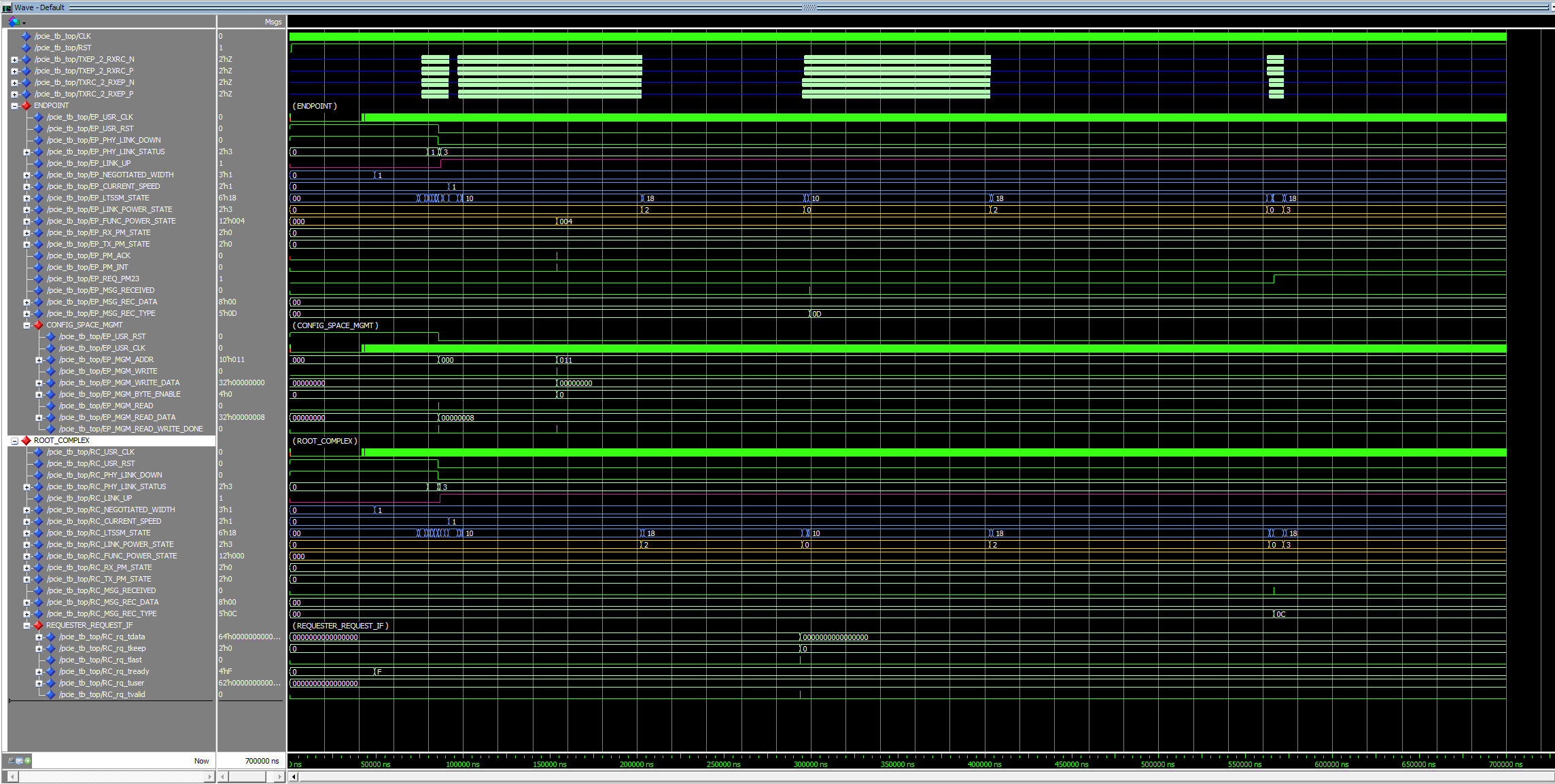
In order to see whether this all works as intended, there is a couple of important signals to watch in the simulation
-
ltssm_state – Shows the associated L0 → L1 → L0 transitions along with initial negotiation during enumeration.
-
function_power_state – Notifies the entry to D3_Hot.
-
link_power_state – shows the actual link state.
- RX Message Interfaces of both RC and EP to see which messages has been received
- NOTE: Messages may be routed to the completer request interface, check that the IP is configured to really forward messages to the RX Message Interface.
I have added a transcript of the simulation, showing only the important parts and transitions.Furthermore, in order to verify that the Config Management Interface works as Intended, I have issued a read transaction to the Type 0 Header with DWORD Address 0x0 (See PG213 “PCI Config Space Header (Type 0 and 1)”) – Vendor ID & Device ID. These numbers may be customized in the Vivado GUI. I did not use the ASPM in this demo, as it is not important. Both PCIe Devices (EP & RC) have been configured to use 2 lanes and up to Gen 2.0 speed (5GT/s).
Simulation Log
# ** Note: EP Function Status: D0_uninitialized
#    Time: 300 ps
# ** Note: EP Link Status : L0
#    Time: 300 ps
# ** Note: EP LTSSM: Detect.Quiet
#    Time: 300 ps
# ** Note: EP LTSSM: Detect.Active
#    Time: 73724200 ps
# ** Note: EP LTSSM: Polling.Active
#    Time: 74676200 ps
# ** Note: EP LTSSM: Polling.Configuration
#    Time: 78168200 ps
# ** Note: EP LTSSM: Configuration.Linkwidth.Start
#    Time: 79512200 ps
# ** Note: EP LTSSM:  Configuration.Linkwidth.Accept
#    Time: 80200200 ps
# ** Note: EP LTSSM: Configuration.Lanenum.Wait
#    Time: 81992200 ps
# ** Note: EP LTSSM: Configuration.Lanenum.Accept
#    Time: 83536200 ps
# ** Note: EP LTSSM: Configuration.Complete
#    Time: 83792200 ps
# ** Note: EP LTSSM: Configuration.Idle
#    Time: 84840200 ps
# ** Note: EP LTSSM: L0
#    Time: 85500200 ps
# ** Note: Successfully read VENDOR ID: 10EE
#    Time: 85820100 ps
# ** Note: Successfully read DEVICE ID: 9022
#    Time: 85820100 ps
# ** Note: EP LTSSM: Recovery.RcvrLock
#    Time: 87872200 ps
# ** Note: EP LTSSM: Recovery.RcvrCfg
#    Time: 88380200 ps
# ** Note: EP LTSSM: Recovery.Speed
#    Time: 91536200 ps
# ** Note: EP LTSSM: Recovery.RcvrLock
#    Time: 96672200 ps
# ** Note: EP LTSSM: Recovery.RcvrCfg
#    Time: 98592200 ps
# ** Note: EP LTSSM: Recovery.Idle
#    Time: 99120200 ps
# ** Note: EP LTSSM: L0
#    Time: 99556200 ps
# ** Note: EP Function Status: D3_hot
#    Time: 153884200 ps
# ** Note: EP Link Status : L1
#    Time: 202516200 ps
# ** Note: EP LTSSM: L1.Entry
#    Time: 202516200 ps
# ** Note: EP LTSSM: L1.Idle
#    Time: 203668200 ps
# ** Note: EP Link Status : L0
#    Time: 296268200 ps
# ** Note: EP LTSSM: Recovery.RcvrLock
#    Time: 296268200 ps
# ** Note: EP LTSSM: Recovery.RcvrCfg
#    Time: 296548200 ps
# ** Note: EP LTSSM: Recovery.Idle
#    Time: 298452200 ps
# ** Note: EP LTSSM: L0
#    Time: 298556200 ps
# ** Note: EP Received: PME_Turn_Off Message
#    Time: 299112200 ps
# ** Note: EP Link Status : L1
#    Time: 403168200 ps
# ** Note: EP LTSSM: L1.Entry
#    Time: 403168200 ps
# ** Note: EP LTSSM: L1.Idle
#    Time: 404308200 ps
# ** Note: EP Link Status : L0
#    Time: 562388200 ps
# ** Note: EP LTSSM: Recovery.RcvrLock
#    Time: 562388200 ps
# ** Note: EP LTSSM: Recovery.RcvrCfg
#    Time: 565044200 ps
# ** Note: EP LTSSM: Recovery.Idle
#    Time: 565564200 ps
# ** Note: EP LTSSM: L0
#    Time: 566000200 ps
# ** Note: RC Received: PME_TO_Ack Message
#    Time: 566400200 ps
# ** Note: EP Link Status : L23 Ready
#    Time: 571904200 ps
# ** Note: EP LTSSM: L1.Entry
#    Time: 571904200 ps
# ** Note: EP LTSSM: L1.Idle
#    Time: 573028200 ps
By default, the PCIe IP doesn’t support sending all kind of messages on the TX Message Interfaces – Which I had hoped for. I had to manually create a PME_TURN_OFF TLP and send it via the AXI RQ interface. At first, I thought that this might be a problem, as constructing a TLP might be a lot of work – But I was really surprised how easy it is to actually sent a Message TLP via the Requester Request (RQ) Interface port on the Root Complex – Basically PG213 tells how to setup a descriptor based on the IP configuration (For my Purpose: PG213 (April 29,2021) : Figure 89) and how to sent the descriptor via the RQ interface (PG213 (April 29, 2021): Figure 45). The hard part is as usual that PG213 doesn’t actually list the required Routing / Message Codes, so that I had to dig a little deep into the base spec to find out:
- PME_TURN_OFF Message Code : “0001_1001”
- PME_TURN_OFF Routing : “011”
The message is sent on the RQ Interface within 2 Cycles in configuration for 64-Bit Interface and 250MHz clock. Caution should also be paid to the option “AXI Stream Alignment mode” – I have used DWORD Aligned. Just note that there are different requirements for the RQ interface operation in different alignment modes! The message is also similar to a posted write, so that there is no need to control the Requester-Completion Interface, which simplifies the TB. I suppose sending a proper memory write / memory read requests might require a little bit more effort, but still I was surprised, that everything worked without any problems thanks to Xilinx’s documentation, which is (Usually) on a very good level. They do ocassionally have bugs, but its nevertheless one of the best written documentations, that I know of. At last, I would also like to point you to the previously mentioned book: PCI Express technology 3.0,which :
Is a must if you are dealing with PCIe of any kind
Finally a few other words – There is an option to use the XDMA IP in the PCIe to AXI Bridge Mode (PG194), which takes care of the RQ/RC/CQ/CC interfaces and manages proper TLP description per the data coming through the AXI4-Channels. It has its drawbacks, as one cannot send an arbitrary message or transaction, but it simplifies the design and one may concentrate on more important tasks. There is even an updated version of the XDMA IP in the “DMA” mode, which includes a DMA (I would guess its the Standard Xilinx DMA connected to AXI4) in order to simplify transfers to and from the core. Since this IP is Encrypted, it takes a bit more time to properly setup the compilation script – Fortunately one may find the Vivado very useful in here – set the project’s simulation tool to modelsim and check the “Generate Simulation Scripts Only” option to create the required compilation and simulation scripts, which one may use to enhance the existing script and add the missing commands and compilation / simulation options easily enough.
The XDMA in the default endpoint configuration (Available for download as .xci at the beginning of this post – Given that it has 2 lanes at Gen 2.0 speed as well as other IPs listed there) properly responds to the PME_TURN_OFF message by sending the PME_TO_ACK message back to the root complex automatically without any user intervention at the bridge side. In this mode (XDMA Endpoint in AXI Bridge Mode), there is no RX Message Interface available, so I was checking the RC’s RX Message Interface only to see whether the PME_TO_ACK Arrives – And It does. This may also be verified in the HDL code by looking at the connection between cfg_power_state_change_ack and cfg_power_state_change_interrupt ports of the PCIe HARD IP located within the XDMA IP container.